
The Hidden Cost of Micron-Level Mistakes
When a U.S. smartwatch brand rejected 25% of a sapphire lens shipment—not for flaws, but because each was 3–7 microns too thick—the delay cost them 11 days of assembly and triggered retail penalties. That kind of error is common: micron-level dimensional deviations cause over 40% of non-cosmetic rejections in wearables, medical devices, and aerospace optics. These aren’t rare failures—they’re systemic, expensive leaks in the production pipeline.
Legacy QA in many sapphire china factories relies on manual micrometers, spot checks, and visual grading. These methods miss subtle warpage and thickness gradients that only show up during thermal cycling or lamination. Worse, physical probes can scratch the very surface they’re meant to protect. Sub-micron deviations mean real-world consequences: delayed launches, scrapped modules, and strained supplier relationships.
ISO 10110 requires ±5µm tolerance on optical-grade sapphire. But a 2024 OpticaTech Insights study found manual inspections miss up to 40% of out-of-spec units. That’s nearly two in five defective crystals passing QA—only to fail downstream. Catching these errors earlier doesn’t just reduce scrap—it prevents cascading delays across global supply chains.
How Non Contact Profilometry Changes the Game
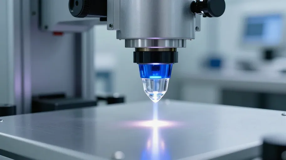
Non-contact profilometry means manufacturers can measure sapphire thickness without touching it, because chromatic sensors or laser interferometry capture data optically. This eliminates mechanical stress that could trigger microfractures in a material with high hardness but low fracture toughness. For teams, that means zero risk of QA-induced damage and the ability to inspect 100% of output, not just a sample.
One Tier 1 factory in Dongguan switched to full-line scanning and saw a 92% drop in post-QA handling defects. That translated to $1.3 million saved annually in scrap and rework. Automating this step doesn’t just improve accuracy—it removes human variability from a process where consistency is everything.
For engineering leads, this shift means fewer surprises during integration. For finance teams, it means lower unit costs and more predictable margins. And for executives, it strengthens supplier credibility in high-stakes contracts where reliability is non-negotiable.
Surface Flatness Mapping That Prevents Assembly Failures
Surface flatness mapping means every wafer gets a full 3D topographical scan, because modern systems capture over 10,000 data points per 100mm disk—far beyond the three-point checks of traditional gauges. This level of resolution reveals bow, warp, and localized curvature invisible to manual tools, which directly impacts compatibility with automated lamination in display stacks.
Even 2µm of unevenness can cause delamination or optical distortion under thermal load. A smartphone OEM that started using mapped specs in procurement saw first-pass yield in display assembly jump from 76% to 94% in six months. That’s not just a quality win—it’s a speed-to-market advantage.
- Full-wafer coverage replaces error-prone sampling with complete data visibility
- Real-time feedback allows immediate tool recalibration, stopping drift before it affects thousands of units
- Digital twin integration enables predictive maintenance of polishing equipment based on actual wear patterns
Beyond Rejection Rates — The Real Business Impact
Preventing one day of assembly line downtime means avoiding $220,000 in lost output and rush logistics (per 2025 Deloitte mobility benchmarks), because automated inspection cells pay for themselves in under two months when they prevent even a single stoppage. But the ROI extends beyond cost savings.
Digital sharing of flatness maps between factory and client means trust replaces dispute. One AR headset maker now receives encrypted reports with every shipment, allowing them to pre-stage assembly parameters instead of waiting for physical validation. That cuts time-to-market by 30%, letting them hit seasonal demand ahead of competitors.
Sapphire isn’t just cover glass anymore—it’s a structural and optical component. Thickness and flatness variations propagate into focus drift, touch errors, and thermal mismatch. By locking in dimensional control at the source, advanced inspection doesn’t just reduce waste. It raises the ceiling for what your product can do.
The Future Belongs to Factories That Measure Smarter
Precision inspection is no longer a back-end cost—it’s a strategic lever for agility, trust, and differentiation. As demand grows for sapphire in foldable displays, LiDAR windows, and biometric sensors, factories that master sub-micron control won’t just pass audits. They’ll set the standard.
The message is clear: if you're sourcing sapphire crystal china factory output without requiring digital dimensional proof, you're betting on luck. The leaders are already shifting to automated, data-driven verification. Ready to stop losing millions to avoidable defects? Start measuring like it matters—because it does.