
Why a Single Micron Can Break a Smartphone Launch
When a leading smartphone maker rejected a shipment of sapphire cover lenses because of a 0.01 mm thickness variation, the fallout wasn’t just scrapped parts—it was a 15-day delay, idle assembly lines, and a dent in investor confidence. That’s because in today’s ultra-thin devices, even microscopic deviations misalign cameras, weaken waterproof seals, or break facial recognition systems. Sapphire crystal dimensional accuracy isn’t optional—it’s the foundation of reliable mass production.
Sub-micron precision means your assembly line runs without constant recalibration because every crystal behaves the same way. This consistency reduces scrap rates by up to 22%, according to TechInsights’ 2024 report on supply chain efficiency. Without it, each batch becomes a unique problem instead of a plug-and-play part.
Chinese manufacturers have shifted from treating metrology as a final gatekeeper to embedding it throughout production. Instead of sampling a few units at the end, they measure every piece at multiple stages—after slicing, grinding, and pre-polishing. This proactive approach catches drift before hundreds of units are compromised. The result? One factory saw first-pass yield jump from 74% to 91% within three months after switching to inline CMMs and laser profilometers.
The Real Reason Most Sapphire Suppliers Fail Final Inspection
Over 60% of premium sapphire vendors outsource final dimensional checks to third-party labs—sometimes days away from their factories. That creates a critical lag: defects are found too late to fix, forcing costly sorting or total rejection. Sampling also misses gradual tool wear or environmental shifts that affect entire batches. You can’t correct what you can’t see in time.
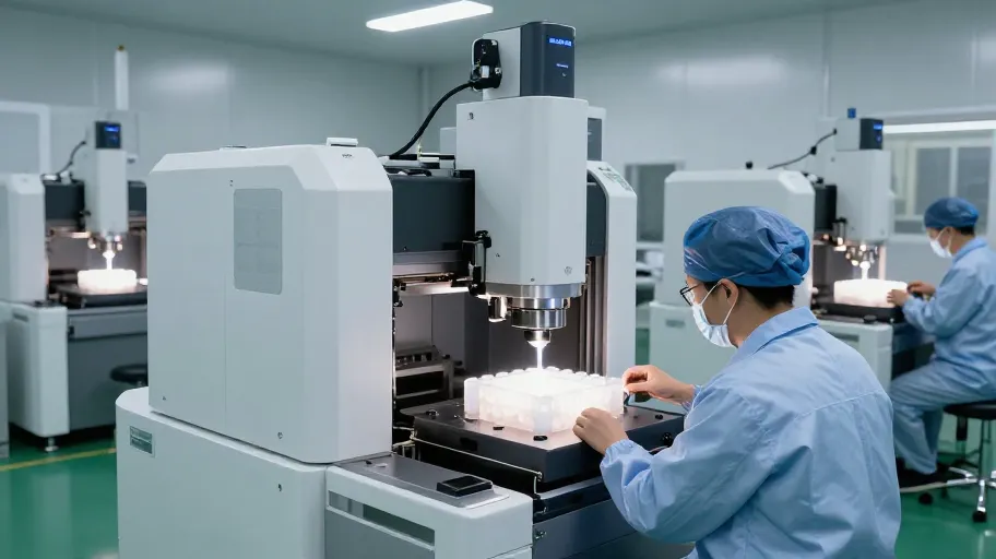
Top Chinese factories solve this by bringing metrology inside the production flow. Inline Coordinate Measuring Machines scan 100% of critical dimensions, while laser profilometers map surface topography at 5-micron resolution. These tools feed data into centralized control systems that adjust CNC polishing heads in real time. If edge thinning starts, pressure profiles auto-correct—no human needed.
This integration means fewer rework cycles, which typically cuts inspection costs by 35%. Full-batch measurement eliminates hidden variation, so downstream OEMs don’t face surprise alignment issues. Digital traceability also enables fast root-cause analysis when problems do arise, accelerating continuous improvement across the line.
How Real-Time Feedback Doubles Yield and Slashes Downtime
One manufacturer reduced rework cycles by 40% after linking automated interferometers directly to CNC polishing cells. By analyzing wavefront data during lapping—not after—it corrected flatness errors before material loss occurred. That shift from reactive to predictive control saved $1.3 million per production line annually.
Automated interferometry means consistent λ/4 surface flatness (about 150 nanometers) across 98.7% of runs, based on SGS testing in 2025. This level used to be exclusive to elite European and Japanese fabs. Now it’s standard in leading Chinese facilities. And because corrections happen mid-process, yield improves without sacrificing speed.
For OEMs, this translates to assembly line stoppages dropping by 68% and calibration downtime falling from 4 hours per shift to under 30 minutes. That kind of predictability is essential for hitting peak-season targets like Black Friday launches. It also protects brand reputation—fewer field failures mean fewer viral videos of cracked screens or blurry photos due to misaligned optics.
Beyond Flatness: Why Internal Clarity Is the Hidden Killer
A sapphire crystal can pass every dimensional test and still fail in the field. Microscopic inclusions, striae from crystal growth, or internal stress zones won’t show up on a CMM—but they become fracture points under thermal cycling or impact. These flaws often emerge only after devices reach customers, turning warranty claims into public relations risks.
That’s why top Chinese factories now combine geometric perfection with structural purity. Advanced polariscopes detect residual stress patterns invisible to the naked eye. High-resolution ultrasound scans identify subsurface inclusions as small as 5 microns. These inspections happen early, so flawed boules are diverted before costly shaping begins.
Catching internal defects early means lower field failure rates—by up to 60% in high-reliability applications like medical devices and aerospace sensors. It also reduces liability exposure for brands using sapphire in mission-critical components. You’re not just buying a dimensionally perfect window—you’re buying long-term reliability backed by science.
From Components to Confidence: The New Standard in Optical Supply
The old model treated sapphire as a commodity—measure some, hope for the best, sort later. The new standard treats it as a precision-engineered system where every micron is accounted for, every defect predicted, and every batch fully traceable. This isn’t overkill—it’s necessity. As phones stack six-lens arrays and AR-ready displays, tolerance budgets shrink to near-zero.
Chinese sapphire factories now deliver more than just material—they deliver manufacturing certainty. When your crystals arrive with certified flatness, verified clarity, and digital inspection logs, your engineers spend less time troubleshooting and more time innovating. Your production teams hit volume targets reliably. Your CFO sees lower scrap, fewer delays, and better margins.
If you're sourcing sapphire for high-density electronics, ask: Does my supplier control metrology—or just outsource it? Do they inspect 100% or sample randomly? Can they prove structural integrity, not just surface specs? Because in the end, true excellence isn’t measured by what you see on the surface—but by what you don’t see beneath it.