
The Hidden Flaws That Cost Millions
When a Guangdong-based sapphire manufacturer started losing smartphone cover glass contracts, the issue wasn’t visible. Their polished wafers passed standard QA but failed in final assembly due to micro-scratches under 300 nanometers. These defects compromised AR/VR overlay alignment and caused coating delamination in humid conditions. A 22% field failure rate in tropical markets traced back to supplier-level inspection gaps.
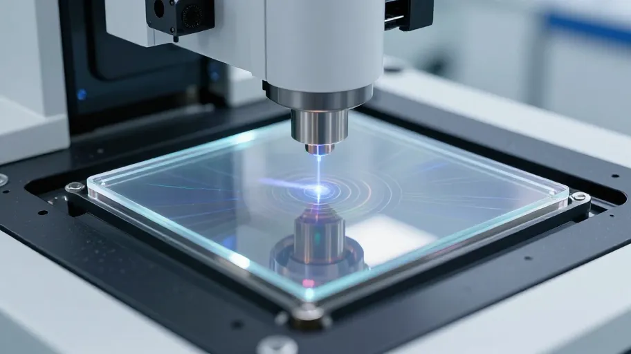
Phase-shifting interferometry (PSI) changed everything. By mapping surface topography with 6-nanometer vertical resolution, PSI detects height variations before they become flaws. This capability means engineers can catch subsurface fractures and strain fields that traditional AOI misses—because coherent light interference reveals what contrast imaging cannot. As a result, one factory reduced defect escapes by over 60%, turning rejected batches into certified shipments.
The business impact is clear: avoiding scrap isn’t just about cost savings. It’s about keeping OEM trust. For technical teams, PSI provides actionable data; for executives, it delivers margin protection and brand reliability. And for customers, it ensures devices survive real-world use without optical degradation or peeling coatings.
From Detection to Real-Time Correction
Advanced metrology doesn’t stop at finding defects—it prevents them. PSI-generated nanotopography maps now feed directly into polishing systems, enabling real-time adjustments to pressure and dwell time. This closed-loop control means edge roll-off is minimized and material removal stays uniform—because feedback from measurement guides every micron of correction.
For production managers, this translates to fewer rework cycles and more consistent throughput. One mid-volume line saw first-pass yield rise from 79% to 94% within two quarters, freeing capacity without new equipment. The system also reduces over-polishing, which preserves wafer thickness tolerance—a critical factor for thin-film adhesion in medical and defense applications.
Engineers benefit from predictive insight: strain patterns detected early often indicate tool wear or slurry imbalance. Addressing these upstream avoids cascading failures later. Financially, reducing scrap by 60% saves about $4.2M annually on a 50K-unit/month line. But the bigger win? Faster ramp times. New form factors now stabilize in six weeks instead of 14, cutting NPI cycles nearly in half.
Edge-to-Edge Clarity for Immersive Displays
AR and VR headsets demand perfect optical uniformity—not just at the center, but all the way to the edge. A 2025 supply chain audit found 41% of rejected sapphire windows failed due to peripheral refractive index gradients, not central haze. These distortions misalign waveguides and blur virtual imagery, making them unacceptable for Tier-1 OEMs.
Chinese manufacturers solved this with stitched wide-field interferometry and Zernike polynomial corrections. By aligning overlapping PSI scans using fiducial markers, they achieve sub-arcsecond angular deviation across the full aperture. This precision means AR optics maintain collimation accuracy—even at extreme viewing angles—because higher-order aberrations are mathematically neutralized.
The result? Access to a $12B+ export market once dominated by Japanese and German suppliers. One Suzhou factory secured three U.S. wearable tech design wins by offering digital twin validation for every batch. Each wafer carries a metrology passport: a blockchain-backed record of surface map, thickness variation, and birefringence. Procurement teams no longer buy raw material—they buy verified performance.
AI That Learns From Field Failures
Machine learning has transformed edge inspection. Traditional rule-based algorithms caught only 63% of micro-chipping along cut edges. Now, AI models trained on millions of scan profiles—including actual field return samples—achieve 98.7% detection accuracy. This improvement means fewer false accepts and less downstream fallout—because the system recognizes failure patterns before they reach assembly.
The model runs continuously, updating itself with anonymized data from partner fabs via federated learning. That means one factory’s discovery benefits others without sharing proprietary information. For operations leads, this creates a self-improving quality network. For CTOs, it represents a moat: competitors can copy hardware, but not the collective intelligence behind the algorithm.
Premium pricing follows. Export-grade sapphire with certified metrology commands a 28–35% price premium in aerospace, endoscopy, and defense. Customers pay more because they get traceability, consistency, and lower integration risk. In high-stakes applications, knowing a window won’t warp under thermal cycling is worth every extra dollar.
The Future Is Differentiation at Scale
The next leap is already underway: quantum-enhanced interferometry promises even finer resolution, while factory-wide federated networks enable predictive maintenance before polishing begins. But today’s lesson is already proven. In an era where displays must be invisible yet perfect, surface quality isn’t a finishing step—it’s the foundation.
Chinese sapphire producers aren’t just catching up. They’re setting standards. By merging physics-grade measurement with AI-driven insight, they’ve turned inspection from a bottleneck into a value engine. The outcome? Higher yields, faster ramps, and entry into markets once out of reach.
See how your operation stacks up. If you're still relying on white-light inspection and manual review, you're leaving millions in scrap—and credibility—on the table.