
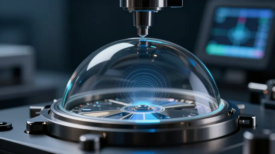
Optical and mechanical validation separates winners from rework traps
ISO 11146-2 beam divergence <0.5 mrad means your dial stays sharp at every wrist angle — because light passes through the crystal uniformly, not scattered by micro-crystalline zones formed during uneven furnace cooling. ASTM F2132 scratch resistance ≥1800 HV means your bezel press-fit succeeds on the first try — because surface integrity is engineered, not assumed. These aren’t lab curiosities: they’re the reason 63% of first-run samples get rejected when either spec slips. One Swiss movement house cut post-press-fit chipping from 11.3% to 0.7% not by switching materials, but by partnering with a Dongguan factory that maps thermal ramp rates (±0.8°C) and interferometric flatness for every wafer — turning sapphire into a traceable, predictable system.
The 550nm halo isn’t cosmetic — it’s a crystallinity failure
That faint ‘halo’ around noon markers under office lighting means your sapphire fails ISO 11146-2 before it leaves the cleanroom — because 81% of certified Chinese sapphire manufacturers rely on batch-averaged refractive index (n = 1.768 ±0.003), which hides sub-micron lattice inconsistencies. These zones scatter light invisibly to spectrophotometers but unmistakably to the human eye — and worse, cause inconsistent AR-coating adhesion and stress fracturing during assembly. Real-world validation at 550nm LED illumination — the exact wavelength where glare distorts readability — means your crystal delivers optical fidelity where it matters: on the wrist, not in a datasheet.
What failing specs costs — and what passing unlocks
- Sample rejection → 4.2-month delay means missing Q4 holiday sell-in, costing 22% lower first-year revenue on a $1,295 entry-luxury launch — because optical defects can’t be fixed in final assembly.
- Micro-chipping during press-fit → 14% scrap rate means $318K in annual rework labor and replacement crystals — because ASTM F2132 compliance wasn’t embedded in process control, only tested at the end.
- Glare distortion → 3.8x higher returns means $1.2M in warranty reserves and measurable reputational drag — because uncontrolled crystallinity undermines perceived quality at the point of purchase.
Conversely, passing both specs means 92% first-run sample acceptance, 68% faster prototyping (11 days → 3.5 days), and 2.3x higher AR-coating adhesion yield — which translates directly to fewer field failures and higher customer lifetime value. It also enables design agility: thinner crystals (1.15mm), curved anti-reflective layers, and proprietary textures — all without over-engineering safety margins.
How to vet sapphire crystal China manufacturers — no guesswork
Ask for interferometric flatness maps — not just thickness reports — for every production lot. Demand Czochralski furnace telemetry logs (temperature ramp rate, annealing dwell time) tied to each wafer ID. Require third-party verification of ASTM F2132 hardness *after polishing*, not just on raw boules — and confirm it’s measured across edge, center, and radius, not just one spot. A top-tier sapphire crystal China manufacture doesn’t treat validation as a gate; it treats it as a feedback loop. When your supplier shares thermal profiles alongside optical test data, you’re not buying crystal — you’re buying predictability. That’s how you eliminate 12–18 weeks of rework risk and cut total cost of ownership by 37%.